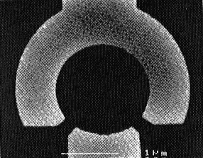
Figure 1. Scanning electron micrograph of a mesoscopic billiard. The white bar at the bottom is 1 micrometer long. The gray area is an electrode deposited on top of a gallium-arsenide semiconductor. A two-dimensional electron gas is formed below the surface (not visible). The electrons can move over the black area but are repelled from the electrode. [From M. J. Berry, J. A. Katine, R. M. Westervelt, and A. C. Gossard, Phys. Rev. B 50, 17721 (1994).]
The quantum billiard is a mesoscopic billiard. Imagine a billiard table which is so small, that one hundred of them would fit on the tip of a needle, and fabricated with such an accuracy that it is completely smooth and flat. Billiard balls shoot over this table with velocities of a hundred miles per second, colliding elastically with the walls until they disappear into one of the pockets. An example of such a billiard is shown in figure 1.
The billiard balls I have in mind are the electrons. You should know that the motion of an electron in a typical metal wire does not resemble at all the rectilinear motion of a billiard ball. The impurities in the metal scatter the electrons in all directions, so that the motion becomes completely unpredictable. One speaks of a "random walk". A measure for the influence of impurities on the electron motion is the socalled "mean free path". This is the typical distance an electron can move before colliding with an impurity. What we need for our game, is a mean free path much greater than the size of the billiard.
The electronic industry has become very skilled at fabricating semiconducting materials (out of which transistors are made) with a large mean free path. The world record is around 100 micrometer. To eliminate the impurities a technique is used called "molecular beam epitaxy". A crystal is grown one atomic layer at the time, until a nearly perfect lattice of atoms is obtained. Because the process is controlled on the atomic scale, it is possible to vary the composition of the individual atomic layers in the crystal. This is used to fabricate a billiard table for electrons which is not only very smooth (i.e. with a large mean free path), but also perfectly flat.

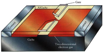
Figure 2. Cross-sectional view of a two-dimensional electron gas (red) at the interface between gallium-arsenide (GaAs) and aluminum-gallium-arsenide (AlGaAs). A gate electrode creates a barrier with a small opening. A current flows through the opening if a voltage is applied between the two contact pads.
The way in which this is done is quite ingenious. The crystal grower varies the composition of the atomic layers in such a way that a potential well for electrons is created inside the material gallium-arsenide. This potential well confines the electrons in the direction perpendicular to the layers, but does not hinder their motion parallel to the layers. One boundary of the well is formed by the interface between gallium-arsenide and the alloy aluminum-gallium-arsenide. The other boundary is formed by the attractive force of positively charged silicon donors in the aluminum-gallium-arsenide. The width of the potential well is only a few atomic layers. In such a narrow well the motion of the electrons perpendicular to the layers is completely suppressed, because the width is smaller than the electron wave length. All motion takes place in the two-dimensional plane perpendicular to the atomic layers. One speaks of a two-dimensional electron gas.
It reminds me of the novel Flatland by Edwin Abbott. In the last century Abbott fantasized about a world where only two spatial dimensions exist. He imagined "a vast sheet of paper, on which straight Lines, Triangles, Squares, Pentagons, Hexagons, and other figures, instead of remaining fixed in their places, move freely about, on or in the surface, but without the power of rising above it, very much like shadows." One hundred years later, this fantasy has become true -- to some extent -- in a two-dimensional electron gas.
There is a problem with this billiard table: the two-dimensional electron gas is buried in the interior of the crystal. How to reach it from the outside? Fortunately, a method exists. The materials gallium-arsenide and aluminum-gallium-arsenide are semiconductors. Unlike a metal, a semiconductor can be deeply penetrated by an electric field. A spatially confined electric field can form a barrier in the two-dimensional electron gas, which repels the electrons in a completely elastic way. Such an electric field is generated by a metal (typically gold) electrode on top of the semiconducting crystal. The electrode is called a "gate". An opening in the gate creates a hole in the barrier, through which electrons can enter and leave the billiard (see figure 2). Using the technique of electron beam litography one can fabricate electrodes with openings of less than 0.1 micrometer. In this way one obtains the micron-sized billiard shown in figure 1.